- 您现在的位置:买卖IC网 > Sheet目录461 > IXTH16P20 (IXYS)MOSFET P-CH 200V 16A TO-247
IXTH 16P20
Symbol
Test Conditions
Characteristic Values
(T J = 25 ° C, unless otherwise specified)
min.
typ.
max.
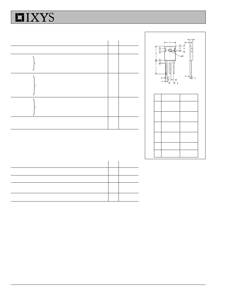
TO-247 AD Outline
g fs
V DS = -10 V; I D = I D25 , pulse test
6
10
S
C iss
C oss
V GS = 0 V, V DS = -25 V, f = 1 MHz
2800
550
pF
pF
1
2
3
C rss
t d(on)
240
33
pF
ns
t r
V GS = -10 V, V DS = 0.5 V DSS , I D = 0.5 I D25
26
ns
t d(off)
R G = 4.7 ? (External)
65
ns
Terminals: 1 - Gate
3 - Source
2 - Drain
Tab - Drain
t f
25
ns
Dim.
Millimeter
Inches
Q g(on)
95
nC
Min. Max.
A 4.7 5.3
Min. Max.
.185 .209
A 1
A 2
Q gs
Q gd
V GS = -10 V, V DS = 0.5 V DSS , I D = 0.5 I D25
27
40
nC
nC
2.2 2.54
2.2 2.6
b 1.0 1.4
.087 .102
.059 .098
.040 .055
R thJC
0.42
K/W
b 1
b 2
1.65 2.13
2.87 3.12
.065 .084
.113 .123
R thCS
0.25
K/W
C .4 .8
D 20.80 21.46
.016 .031
.819 .845
E 15.75 16.26
e 5.20 5.72
L 19.81 20.32
L1 4.50
? P 3.55 3.65
Q 5.89 6.40
.610 .640
0.205 0.225
.780 .800
.177
.140 .144
0.232 0.252
Source-Drain Diode
Characteristic Values
(T J = 25 ° C, unless otherwise specified)
R 4.32 5.49
S 6.15 BSC
.170 .216
242 BSC
Symbol
Test Conditions
min.
typ.
max.
I S
I SM
V SD
t rr
V GS = 0
Repetitive; pulse width limited by T JM
I F = I S , V GS = 0 V,
Pulse test, t ≤ 300 μ s, duty cycle d ≤ 2 %
I F = I S , di/dt = 100 A/ μ s, V R = -50 V
250
-16
-64
-3
A
A
V
ns
IXYS reserves the right to change limits, test conditions, and dimensions.
IXYS MOSFETs and IGBTs are covered by one or more
4,835,592 4,881,106 5,017,508 5,049,961 5,187,117 5,486,715 6,306,728B1 6,259,123B1 6,306,728B1
of the following U.S. patents:
4,850,072 4,931,844 5,034,796 5,063,307 5,237,481 5,381,025 6,404,065B1 6,162,665
6,534,343 6,583,505
发布紧急采购,3分钟左右您将得到回复。
相关PDF资料
IXTH180N10T
MOSFET N-CH 100V 180A TO-247
IXTH182N055T
MOSFET N-CH 55V 182A TO-247
IXTH200N085T
MOSFET N-CH 85V 200A TO-247
IXTH200N10T
MOSFET N-CH 100V 200A TO-247
IXTH20N60
MOSFET N-CH 600V 20A TO-247AD
IXTH220N055T
MOSFET N-CH 55V 220A TO-247
IXTH220N075T
MOSFET N-CH 75V 220A TO-247
IXTH230N085T
MOSFET N-CH 85V 230A TO-247
相关代理商/技术参数
IXTH16P60P
功能描述:MOSFET -16.0 Amps -600V 0.720 Rds RoHS:否 制造商:STMicroelectronics 晶体管极性:N-Channel 汲极/源极击穿电压:650 V 闸/源击穿电压:25 V 漏极连续电流:130 A 电阻汲极/源极 RDS(导通):0.014 Ohms 配置:Single 最大工作温度: 安装风格:Through Hole 封装 / 箱体:Max247 封装:Tube
IXTH17N55
制造商:未知厂家 制造商全称:未知厂家 功能描述:TRANSISTOR | MOSFET | N-CHANNEL | 550V V(BR)DSS | 17A I(D) | TO-218VAR
IXTH17N60
制造商:未知厂家 制造商全称:未知厂家 功能描述:TRANSISTOR | MOSFET | N-CHANNEL | 600V V(BR)DSS | 17A I(D) | TO-218VAR
IXTH17N65
制造商:未知厂家 制造商全称:未知厂家 功能描述:TRANSISTOR | MOSFET | N-CHANNEL | 650V V(BR)DSS | 17A I(D) | TO-218VAR
IXTH17P25
制造商:未知厂家 制造商全称:未知厂家 功能描述:TRANSISTOR | MOSFET | P-CHANNEL | 250V V(BR)DSS | 17A I(D) | TO-218VAR
IXTH180N085T
功能描述:MOSFET 180 Amps 85V 5.5 Rds RoHS:否 制造商:STMicroelectronics 晶体管极性:N-Channel 汲极/源极击穿电压:650 V 闸/源击穿电压:25 V 漏极连续电流:130 A 电阻汲极/源极 RDS(导通):0.014 Ohms 配置:Single 最大工作温度: 安装风格:Through Hole 封装 / 箱体:Max247 封装:Tube
IXTH180N10T
功能描述:MOSFET 180 Amps 100V 6.1 Rds RoHS:否 制造商:STMicroelectronics 晶体管极性:N-Channel 汲极/源极击穿电压:650 V 闸/源击穿电压:25 V 漏极连续电流:130 A 电阻汲极/源极 RDS(导通):0.014 Ohms 配置:Single 最大工作温度: 安装风格:Through Hole 封装 / 箱体:Max247 封装:Tube
IXTH182N055T
功能描述:MOSFET 182 Amps 55V 4.4 Rds RoHS:否 制造商:STMicroelectronics 晶体管极性:N-Channel 汲极/源极击穿电压:650 V 闸/源击穿电压:25 V 漏极连续电流:130 A 电阻汲极/源极 RDS(导通):0.014 Ohms 配置:Single 最大工作温度: 安装风格:Through Hole 封装 / 箱体:Max247 封装:Tube
